 |
| ESD Technical e-Newsletter |
|

|
Feb 2001
Issue 2, Volume 4
|
|
IC LOGIC SUSCEPTIBILITY FROM ESD INDUCED EM RADIATION
| |
Often unanticipated, ESD is a potential source of EMI. A significant ESD event will generate a high-energy pulse EMI that can be destructive to neighboring electronic systems. This can manifest itself in the form of logic error conditions including data errors, systems lock-ups, software errors, and robotic malfunctions, etc.
INTRODUCTION
Current Electrostatic Discharge (ESD) control practices have substantially minimized the dangers from unwanted electrical overstresses that are known to haunt semiconductors and other micro-electrical devices at all stages of their manufacturing, handling and applications.
The act of grounding an ungrounded ESD Sensitive (ESDS) device can trigger an ESD event, yielding latent or catastrophic damage by means of an energy or voltage failure mechanism in the ESDS device. To minimize this potential problem, the rate of discharge must be controlled during grounding and the work potential at the grounding electrode must be increased [1]. Decreasing the rate of discharge will limit the current density of a potential electrical arc (ESD event). Any combination of an increase in resistance or capacitance in the contacting electrodes (the two materials that sustain a discharge) can decrease the rate of discharge and lessen the effects of an ESD Event.
One of the side effects from electrostatic discharge (ESD) is an induced EMI. An ESD-induced EMI in the near-vicinity of mission-critical equipment can cause data errors, temporary resets or even power-up resets requiring operator intervention [2]. This is caused by the EMI undergoing conversion to a voltage or current, which in turn corrupts the operation of the circuit/logic inputs.
The effects from undesired electromagnetic radiation, EMI, on ungrounded or unshielded conductors is commonly underestimated. An ESD event occurring outside an ESDS protective work area can still pose a risk to unshielded and ungrounded conductors within the critical work or ESDS area.
CASE EXAMPLES
Some examples of ESD/EMI problems reported from the Center for Devices and Radiological Health (CDRH) databases are listed by product recall numbers. Recall numbers M485337, M485338, M562311, March 1994, states that static from bed sheets when a nurse was making the bed caused infusion pumps to sound a "processor lock-up alarm". Recall number M249358, October 1991, states that a discharge from an operator to the timer of a radiation therapy system caused the timer's display to blank just as treatment began. Recall numbers Z3112, Z3212, Z3132, Z142, January 1992, states that ESD affected infant radiant warmers, causing the heater to turn on or off, the alarm not to activate, and the display to become blank or corrupted, [9].
Today's TTL and CMOS logic states have a logic "0" at 0.8 Volts or lower and a logic "1" at 2.0 Volts or higher. This leads to a smaller indeterminate range of 1.2 Volts for most TTL and some CMOS logic circuits and places the logic inputs from these circuit traces or cable connections susceptible to induced EMI voltages exceeding this range. One example of an ESD-induced EMI was characterized from office chairs [3, 4]. Induced voltages over 2 Volts have been measured on a printed circuit assembly (PCA) 90 cm from the furniture ESD [4]. Two Volts is enough voltage to easily drive a TTL circuit let alone an ECL circuit into a logic error.
Table I lists some logic devices, and their potential susceptibility to EM energies. Noise margin is a quantitative measure of a device's noise immunity. The high level DC noise margin in Table I is the difference between the minimum device output levels for a logic high VOH of the driving gate and the minimum input level VIH required by the driven gate to recognize a "1" logic state. The Indeterminate Range is the difference between the logic inputs' low level maximum and high level minimum to differentiate between a logic "0" or "1".
Some types of common lab stools and office chairs can radiate a series of impulsive fields from metal legs due to internal ESD when a person rises from the chair. As many as 12 pulses have been recorded within a 10 second period after a person rises from a chair [3].
Smith stated that a value of tens of millivolts per inch (~2 V/m) is generally not enough to affect digital logic whereas values over one volt/inch (40 V/m) are potential problems. One example observed induced voltages of over 4 volts/inch (>160 V/m) in cables one foot from one type of office chair [3].
Table I
Table of Logic Families' Power Transition, Noise Margin, and Indeterminate Range
|
Logic Family
|
Static Power Dissipation per gate (mW) |
High Level DC Noise Margin (mV) |
Input Logic Indeterminate Range (V) |
|
ECL-10 |
25 |
145 |
0.37 |
|
TTL |
10 |
400 |
1.2 |
|
ALS-TTL |
1.2 |
500 |
1.2 |
|
AS-TTL |
2 |
500 |
1.2 |
|
LS-TTL |
2 |
500 |
1.2 |
|
HC-CMOS |
0.003 |
175 |
2.25 |
|
HCT-CMOS |
0.003 |
165 |
1.2 |
What often looks like software errors in process equipment may actually be caused by an external static charge (or discharge) problem. An ESD event anywhere in a room can cause an EMI. That EMI can couple into a system through cables or open chassis and induce a noise voltage greater than the logic inputs' indeterminate range and cause a single event upset. EMI effects to microprocessors or other circuit logic latch-ups in process equipment can manifest itself in a number of ways, such as random hangs, robotic malfunction, or software errors, all resulting in downtime and reduced throughput.
THEORETICAL ENERGY ANALYSIS
MECHANISM OF AN ESD EVENT
There are three well-known methods to simulate an ESD Event: the human body model, the machine model and the charge device model. Each has its place to aid in designing the proper ESD Control Program depending on the application.
Induced voltage from an EMI energy transfer to a logic input trace with typical area of 40 mm2 could be as high as 485 mV with an ESD-induced 100 MV/m field at 33 cm as depicted in Table II. 485 mV is enough voltage to flip a logic state of an ECL device as depicted in Table I. From the same ESD event, a data input cable with a receiving area of 40 cm2 can have an EMI-induced voltage of 4.85 which is enough voltage to drive a logic error in any family or subfamily of logic circuits; TTL, CMOS, & ECL.
Table II
EMI Energy Transfer from an ESD to an Isolated Conductor using antenna theory where: the area of the conductor is A=variable, the distance from the source is R=1/3 meter, ESD has a 1 ns rise time and a 3 ns pulse width.
|
Field Strength
From ESD Event |
Induced Voltage on Receiving Area |
|
E (V/m) |
40 mm2 |
4 cm2 |
40 cm2 |
400 cm2 |
0.4 m2 |
|
100 MV/m |
485 mV |
1.53 V |
4.85 V |
15.3 V |
48.5 V |
|
1 MV/m |
4.85 mV |
15.3 mV |
48.5 mV |
153 mV |
485 mV |
|
1 KV/m |
4.85 m V |
15.3 m V |
48.5 m V |
153 m V |
485 m V |
ESD EVENT
An ESD event can have a fast rise time, especially for low voltage discharges [5]. The waveform for an ESD event includes high-frequency components with a frequency range from DC to over 6 GHz, [4]. This electromagnetic radiation (EM) can readily couple to circuit traces (conductors acting as antennae). For ungrounded conductors coupled within a capacitive circuit, this EM wave can induce a static charge, building until a discharge, breakdown, recombination, or neutralization occurs. High-speed circuits, by their nature, tend to be very susceptible to high-frequency signals such as those from a nearby ESD event.
The electrostatic field strength (Eo) just before an ESD is proportional to the charged voltage (V) at gap width gamma . The gap width, gamma , is defined by Paschen's Law, but may vary in each discharge condition. The electric field strength Eo = V/gamma where V is from 0.5 kV to 30 kV and gamma is from 5 micro meters to 10 mm can yield an electric field strength as high as 6 GV/m. This extremely high field strength is attributed to a smaller gap width, gamma = 5 micro meters. It is important to note that the arc length of an ESD is of greater influence to its disturbance than its voltage [7].
EMI
An Electromagnetic Interference (EMI) is an unwanted electromagnetic energy, (whether intentionally or unintentionally generated), of almost any frequency and energy level. EMI is defined to exist when undesirable voltages or currents are present to adversely influence the performance of an electronic circuit or system. Sources of radiated electromagnetic energy from ESD are very common in today's factories from furniture ESD, raised flooring ESD, Human Body ESD, hand held toolbox ESD and metal-to-metal ESD [3, 4, 6, 7]. An EMI, or summation of EMIs, can over time induce a charge (static voltage) on an ungrounded conductor coupled in a capacitive circuit, i.e., an isolated capacitor. An even more common occurrence is a single ESD induced EMI that can upset a logic circuit and cause systems errors. The very fast rise time of an ESD may be preserved if it flows through a metal conductor, resulting in radiated EMI.
SOME SOLUTIONS
Assume that all electronic devices are susceptible to damage or logic error states from ESD and EMI, respectively; and take the proper precautions.
Proper grounding of isolated conductors and use of ground-planes near active conductors will minimize some of these effects.
Shielding the known emitting devices will help, but it is the unknown emitters that will cause the most problems. Thus, shielding the receptors, sensitive logic devices, will help combat EMI-induced logic errors. Start shielding at the device level, for it is less costly than at the system level.
Reduce ground-loop areas between interconnected equipment and systems. Route interconnected cables inside conduit, cable trays or raceways when possible. Do not coil excess cable into a helix, but rather fold back and forth to foil antenna gains.
Metal-to-metal discharges will always derive the largest current derivatives (di/dt) and hence generate the strongest EMI fields. Treat isolated conductors as charged devices and ground them with an electrically dissipative material (R > 10^4 Ohms ). This will slow down the energy transfer from the conducted ESD causing the resultant EMI to be negligible to any active near or far field system.
CONCLUSION
A high energy ESD can drive a substantial EMI energy to couple and charge passive circuits or energize active circuits with significant system problems. EMC practices involving shielding designs typically account for EMI from known sources, but should also consider unplanned sources such as ESD events in the near vicinity of the active or sensitive system(s).
With today's logic devices having smaller noise margins and indeterminate ranges, susceptibility to ESD-induced EMI should be accounted for in the design and implementation of the systems incorporating logic circuits.
Refer to our white paper for references
|
|
|
|
|
|
|
|
|
|
|
|
|
Product document support includes a technical brief, drawing or bulletin. These are referenced within our on-line catalog as well as listed in our web site.
|
|
|
|
Certification Information
|

|

|
|
|
|
|
Extra Protection
|
|
For added protection, ESD Systems.com branded personal grounding products are packaged in antistatic low charging bags which are indicated as ESD protecting by the inclusion of the ESD Protective Symbol as Per S8.1 paragraph 4.1.
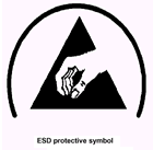
When stocked in the "Kitting" rooms we supply a complete package that is ESD protective. Remember that the ESD protective symbol should also be used on items designed to replace static generative materials. This provides added peace of mind when bringing in an ESD Systems.com Wrist Strap/Foot Strap/Ground cord into an ESD Protected Area as packaged vs products that are packaged in regular high charging plastic bags.
.
|
Auto Calibration Unit
Item #43469
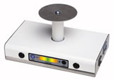
- Auto Calibration Unit for the CE Ionizer
- Calibrates the CE Ionizer in under 60 seconds right at the workstation
- Has closed loop calibration circuit to calibrate the ESD Systems.com CE Ionizer to the changing conditions at the worksurface
- Minimize workstation down time, e.g., the ionizers will not have to be returned to the metrology lab or manufacturer factory for calibration
- Calibration unit derives power from the ionizer under test
- Provides a visual balance indicator that displays the ionizer balance level
Buy Now  Tech Info
|
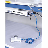
NEW!
XL Bench Top Ionizer
Item #43106

- Features a patented Faraday balance system that automatically maintains a balanced ion output and also emits ions in a true laminar flow, which reduces ion recombination and emitter contamination
- AC ionizing system for superior performance in neutralizing static charges at greater distances
- Non-nuclear operation for added safety
- Gold plated emitters for longer life
- Fixed temperature heater that removes chill from air and enhances worker comfort and productivity
- Multiple installation options that provides flexibility
- Ground point for personnel grounding
Buy Now
|
|
|
|
|
|
Product document support includes a technical brief, drawing or bulletin. These are referenced within our on-line catalog as well as listed in our web site.
|
|
|
|
|
|
|
|
Q56: Static shocks are rebooting computers at 17 - 20 feet away during the winter months (seems like when heat is on). Have you heard of this? (I need data 'proof' that this can cause damage at distances) What product solutions do you have? - Anonymous, Fort Polk, LA see ANSWER 56
Q359: How are the electronics inside plastic cell phones and hand held computers protected from externally generated electrostatic fields? -Anonymous, Elkhorn, Wisconsin see ANSWER 359
Q481: We have two buildings in our campus. One building has got Antistatic tile, but the other one doesn't. We develop Computer software and keep lots of computer and other networking equipments which is required for software development. We are experiencing lot of static problems in the building where we do not have antistatic carpet. Could you inform us in detail how does this affect computer suystems? We are planning to change the carpet to Anti static capet tiles. We would like to know in detail how does this effect computer and other related networking equipments? What might go wrong (parts) in the equpment because of static current? Suresh, Bangalore, India see ANSWER 481
Q529: We have one customer with Fast Ethernet Network (with Pentium III 500 Mhz Clone Pc´s, connected by UTP cable, total 15 pc´s) in Mexico City and they have Electric Contacts without Physic ground and they have carpet on the floor of all the office. In this moment they don´t have a significant problems and for this they wish not change this situation. I want ask you. Is it a big problem (on the future)? Exist some rule or specification about this? What problems can have the costumer with your network or pc´s? - Agustín Ramírez, Ingeniería Asociada S.A., Mexico see ANSWER 529
Q651: I am working on a product that uses mild electrostatics to attract and trap dirt. Basically it is a cloth that resembles paper towels that you wipe over furniture, countertops and electronics in your house to remove dust from them. I was wondering if there are standards and specs stating the average amount of electrostatic charge an average TV, VCR, car radio, telephone, etc. can take before getting shorted? -Nirav Shah, Cincinnati, Ohio see ANSWER 651
|
|
|
|
NOTE:
If you haven't already done so, downloading Acrobat Reader is highly recommended as most of our Technical Literature is in an electronic form known as portable document files (PDF). These can be eMailed or downloaded from our website, however you'll need Adobe Acrobat Reader to view them.
The good news is that this program is free. Adobe Acrobat can be downloaded from Adobe's website. The file is over 3 megs, so be sure you have the capacity to receive that large a file.
|
|
|
|
|
|
ANSI/ESD-S20.20 Regarding Floors and ESD-STM97.2 1999
Statproof® Zinc Free Dissipative Floor Finish and Statproof® Conductive Paint can dissipate a charge of 5,000 volts to zero in 10 ms without the need for external grounding when the treated surface exceeds about 20 square feet. The logic behind this can be explained using field theory, but a simpler explanation can be used when simplifying field theory into lumped circuit theory.
The treated surface becomes a huge capacitor, similar to a parallel plate capacitor. The simplified equation for capacitance in this situation is the capacitance (C) is equal to the area (A) multiplied by the dielectric constant (e) all divided by the spacing between the substrate and paint (d).
C = eA/d
Let's assume that the dielectric constant of the material is unity (1) for this case (which is the approximate dielectric constant for air....so the total dielectric constant is just 8.85x10^-12 F/m), and the spacing (film thickness) is 2 mils, so the capacitance for a 20 square feet Statproof® surface is 6,474 microfarads. Typical human body capacitance is 50 to 150 picofarads or about 65,000 times smaller than the treated floor. Due to this inbalance, a charge residing on the human body (say 5,000 volts) will be neutralized (sucked away) very quickly (much less than a second ~ 0.01 seconds) because the floors capacitance is HUGE in comparison to the human body or other charged objects that may come into contact with the floor.
The following analogy may prove useful........imagine that the painted floor is Lake Erie and the charged human is a glass of water. First measure the depth of Lake Erie, then pour the glass of water into it, now measure it again......see any changes? Probably not, because the Lake is so HUGE in comparison to the glass of water. Same with the floor accepting the charge imbalance of the human body, after neutralizing the body, the floor still appears at zero volts.....or virtual ground.
|
|
|
|
|
|
|
This is a free monthly eNewsletter, which specializes on issues in electrostatic control in the semiconductor/electronics workplace and is best viewed while connected to the Internet.
Let us know what you think. Tell us what you would like to see in future issues. Want to contribute articles or other related information to our Newsletter? If you have any comments, suggestions or feedback about this eNewsletter, please send them directly to the editor@esdsystems.com, Thanks.
|
|
|
Copyright © 2001 ESD Systems.com. All rights reserved.
|
|